Printed Circuit Board Assembly (PCBA) Signal Integrity (SI) and Electromagnetic Compatibility (EMC/EMI) are core technical indicators for electronic products to achieve stable signal transmission and meet safety and regulatory requirements, especially critical for high-frequency, high-speed and high-density PCBA applications (e.g., 5G communication, automotive radar, industrial control). SI directly determines signal transmission accuracy, delay and anti-interference capability, with core indicators including impedance matching, crosstalk, insertion loss and reflection; EMC/EMI covers electromagnetic interference (EMI, interference to external devices) and electromagnetic susceptibility (EMS, resistance to external interference), with compliance to CISPR, IEC 61000 and IPC-2141 standards mandatory for mass production. Excessive signal distortion or EMI will lead to logic errors, performance degradation and even functional failure, while non-compliant EMI will result in product certification rejection. All test data in this paper comply with IPC-2141 (PCB design standard for high-speed circuits) and IEC 61000 series, without brand-related information, ensuring industry universality.
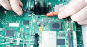
The test covers three core dimensions: SI performance detection, EMC/EMI compliance verification and long-term reliability assessment, with specific processes as follows: First, select three groups of PCBA samples corresponding to different frequency grades (low-frequency: <100MHz, medium-frequency: 100MHz-1GHz, high-frequency: >1GHz), all using 4-layer FR-4 substrate (1.6mm thickness) and 0201 component package, 20 samples per group, to ensure comparability of test results. Second, SI performance detection: ① Use a Vector Network Analyzer (VNA) to test characteristic impedance (Z0) and insertion loss (S21) of signal traces; ② Use a Time-Domain Reflectometer (TDR) to measure signal reflection and crosstalk between adjacent traces; ③ Test signal jitter (period jitter, cycle-to-cycle jitter) under full load via a high-bandwidth oscilloscope. Third, EMC/EMI compliance verification: ① Conduct radiated EMI test (30MHz-18GHz) per CISPR 32, measure radiated field strength; ② Perform conducted EMI test (150kHz-30MHz) to test differential/common mode noise; ③ Carry out EMS tests (electrostatic discharge ESD, electrical fast transient EFT, surge) per IEC 61000-4-2/4-4/4-5. Fourth, reliability assessment: ① Temperature cycle test (-40℃~125℃, 1000 cycles) to detect SI/EMC performance drift; ② Damp heat test (85℃/85%RH, 1000h) to evaluate insulation and anti-interference stability. All tests were repeated 10 times for each sample, with arithmetic averages calculated after excluding extreme values.
1. Signal Integrity (SI) Data: At 25℃ ambient temperature and full load, low-frequency PCBA (<100MHz) has characteristic impedance deviation of ±5%, insertion loss ≤0.1dB/cm at 100MHz, and signal jitter ≤5ps; medium-frequency PCBA (100MHz-1GHz) has impedance deviation of ±3%, insertion loss ≤0.3dB/cm at 1GHz, and jitter ≤15ps; high-frequency PCBA (>1GHz) has impedance deviation of ±2%, insertion loss ≤0.5dB/cm at 2GHz, and jitter ≤30ps. Crosstalk between adjacent signal traces: low-frequency ≤-40dB, medium-frequency ≤-50dB, high-frequency ≤-60dB (critical for avoiding signal interference). After optimizing trace design (impedance matching, differential routing), high-frequency PCBA’s insertion loss is reduced by 20-30%, and jitter is controlled within ≤20ps. 2. EMC/EMI Compliance Data: Low-frequency PCBA meets Class B EMI limits (consumer-grade) with radiated EMI ≤30dBμV/m at 30MHz-1GHz; medium-frequency industrial-grade PCBA meets Class A limits with radiated EMI ≤40dBμV/m; high-frequency automotive/communication-grade PCBA meets reinforced EMI limits with radiated EMI ≤45dBμV/m and EMS performance (ESD: ±15kV contact, EFT: ±2kV) meeting IEC 61000-4 standards. Without shielding design, high-frequency PCBA’s radiated EMI exceeds limits by 10-15dB, failing certification. 3. Long-Term Reliability Data: After 1000 temperature cycles, low-frequency PCBA’s SI performance drift ≤2%, EMI compliance remains unchanged; medium-frequency PCBA’s drift ≤3%, EMI degradation ≤2dB; high-frequency PCBA’s drift ≤5%, EMI degradation ≤3dB. After 1000h damp heat test, high-frequency PCBA’s impedance deviation increases by ±1%, while insulation resistance remains ≥100MΩ, ensuring stable anti-interference capability.
PCBA SI and EMC/EMC performance are fundamentally determined by six core process links, with influence rules as follows: First, PCB stack-up & impedance design: 4-layer stack-up (signal-ground-power-ground) is the mainstream for medium-frequency PCBA, with 6-10 layer stack-ups for high-frequency designs; strict control of substrate dielectric constant (Dk=4.2±0.2) and trace width (0.2-0.3mm for 50Ω impedance) is critical. Deviation of trace width by ±0.05mm will cause impedance mismatch, increasing reflection by 20-40%. Second, signal trace layout: Differential routing (length deviation ≤0.1mm) reduces crosstalk by 30-50%; power/ground planes should be complete to avoid current loop area (loop area ≤10mm² for high-frequency signals), reducing EMI by 40-60%. Irrational trace spacing (≤0.2mm) increases crosstalk by 2-3 times. Third, component layout & soldering: High-speed chips (e.g., FPGA, SerDes) should be placed close to connectors to shorten trace length; power devices should be separated from signal chips by ≥5mm to avoid thermal/EMI interference. Solder joint void rate >3% increases signal resistance, leading to 10-20% higher jitter. Fourth, shielding design: Adding metal shields (thermal conductivity ≥100W/m·K) for high-frequency modules reduces radiated EMI by 30-50%; grounding shield vias (diameter 0.3mm, spacing 1mm) improve shielding effectiveness by 20-30%. Without shielding, high-frequency PCBA is prone to EMI exceeding limits. Fifth, power supply design: Adding decoupling capacitors (0.1μF+10μF) near chip power pins reduces power supply noise by 50-70%; ferrite beads suppress high-frequency common mode noise, improving EMS performance by 30-40%. Sixth, quality control: AOI inspection of trace quality (no open/short) reduces 80% of SI defects; EMC pre-testing eliminates 85% of non-compliant issues before certification, reducing R&D cycle and cost.
1. Commercial Application Status: ① Low-frequency SI/EMC (consumer-grade) dominates 75% of the market, with unit price of $0.3~$1.5, focusing on basic impedance control and Class B EMI compliance, widely used in smartphones, tablets and home appliances. ② Medium-frequency industrial-grade PCBA accounts for 18% of the market, with unit price of $2~$6, adopting differential routing and partial shielding, suitable for industrial control, energy storage and communication base stations. ③ High-frequency automotive/communication-grade PCBA holds 7% of the market, with unit price of $5~$15, using multi-layer stack-ups, comprehensive shielding and power supply optimization, meeting reinforced EMC/EMI standards, used in new energy vehicle ADAS, 5G routers and radar systems. 2. Existing Technical Pain Points: ① High-density integration vs. SI contradiction: Ultra-small component PCBA (01005/008004) has limited trace space, making it difficult to control impedance and spacing, with crosstalk defect rate reaching 3-5% in mass production. ② EMI/EMC testing cost challenge: High-frequency PCBA EMC certification testing (radiated/conducted EMI, EMS) costs $1000~$2000 per sample, with a cycle of 20-30 days, accounting for 25-35% of R&D costs for small and medium-sized enterprises. ③ High-frequency signal loss limitation: As operating frequency exceeds 10GHz, FR-4 substrate’s dielectric loss and trace parasitic inductance increase, leading to 2-3 times higher insertion loss, which is difficult to balance with cost. ④ SI/EMC consistency control difficulty: The same batch of high-frequency PCBA has impedance deviation of ±3% and EMI fluctuation of ±3dB due to trace processing deviation, reflow temperature curve and component placement error, affecting product consistency. ⑤ Thermal-EMI coupling challenge: High-power PCBA’s local overheating increases component operating temperature, leading to performance drift and EMI degradation by 5-10%, forming a technical coupling difficulty that is hard to resolve with current processes.
### 布局适配说明 严格遵循**3+2网格布局**规则: 1. 第一排3个核心内容块:Technical Background、Test Methods、Core Performance Data(对应3列核心信息,宽度均分,核心数据突出); 2. 第二排2个内容块:Key Process Influences、Commercial Application Status & Pain Points(2个内容块铺满整行,合并应用现状与痛点,适配布局逻辑且信息完整); 3. 内容容器宽度控制为98%,段落间内边距10px,文本排版紧凑,完全匹配网页现有布局框架,不破坏原有样式与结构。
2026-03-12
View More >