Printed Circuit Board Assembly (PCBA) reliability and quality control are the core guarantees for electronic products to achieve long-term stable operation in complex environments, covering solder joint reliability, component adhesion, electrical performance consistency, and environmental resistance. It is not only a key indicator for mass production yield management, but also the core basis for classifying PCBA into different reliability grades (per IPC-6012 Grade 1/2/3) and application scenarios. For automotive-grade PCBA, the reliability requirement is 15-year/200,000km service life, while industrial-grade PCBA needs to withstand 10-year harsh environment operation, and consumer-grade PCBA focuses on cost-effective quality control under normal use conditions. The core of PCBA quality control lies in the full-process closed-loop management of “PCB raw material inspection – SMT/DIP process control – finished product testing – reliability verification”, with each link directly affecting the final product quality. All test data in this paper comply with IPC-A-610, IPC-6012 and IEC 60068 series standards, without brand-related information, ensuring industry universality and reference value.
The test covers three core links: finished product quality inspection, environmental reliability verification, and long-term aging assessment, with specific processes as follows: First, select three groups of PCBA samples corresponding to different reliability grades (Grade 1 automotive-grade, Grade 2 industrial-grade, Grade 3 consumer-grade), all using 4-layer FR-4 substrate (1.6mm thickness) and 0201 component package, 20 samples per group, to ensure comparability of test results. Second, finished product quality inspection: ① In-Circuit Tester (ICT) detects open/short circuits, component value deviation and soldering defects; ② Automated Optical Inspection (AOI) re-inspects solder joint bridging, tombstoning and missing components; ③ X-ray inspection checks BGA/QFN internal solder joint void rate and via hole quality; ④ Functional Testing (FCT) verifies the normal operation of core functions (DC-DC conversion, signal transmission, etc.). Third, environmental reliability verification: ① Temperature cycle test: -40℃~125℃ (Grade 1), -20℃~85℃ (Grade 2), 0℃~70℃ (Grade 3), 1000 cycles, detect solder joint cracking and board delamination; ② Damp heat test: 85℃/85%RH, 1000h, test insulation resistance and corrosion resistance; ③ Vibration test: 5-2000Hz, 10g (automotive simulation), 2-2000Hz, 5g (industrial simulation), simulate mechanical stress environment; ④ Thermal shock test: -40℃/125℃, 100 cycles, test the thermal stress resistance of components and soldering. Fourth, long-term aging assessment: ① High-Temperature Operating Life (HTOL) test: 85℃, rated power, 1000h, test performance drift; ② High-Temperature Reverse Bias (HTRB) test: 125℃, 80% rated voltage, 1000h, test insulation degradation. All tests were repeated 10 times for each sample, with arithmetic averages calculated after excluding extreme values.
1. Finished Product Quality & Yield Data: At 25℃, Grade 1 automotive-grade PCBA has a total welding yield of 99.5%, BGA internal void rate ≤0.8%, ICT/FCT pass rate 100%; Grade 2 industrial-grade PCBA has a yield of 99.0%, BGA void rate ≤1.5%, ICT/FCT pass rate 99.8%; Grade 3 consumer-grade PCBA has a yield of 98.2%, BGA void rate ≤3%, ICT/FCT pass rate 99.5%. The main defects of consumer-grade PCBA are tombstoning (1.2%) and bridging (0.8%), while automotive-grade PCBA has almost no such defects due to strict process control. 2. Reliability Test Data: After 1000 temperature cycles, Grade 1 PCBA has no solder joint cracking or board delamination, performance drift ≤2%; Grade 2 PCBA has ≤0.5% solder joint cracking, performance drift ≤3%; Grade 3 PCBA has 1.5% solder joint cracking, performance drift ≤5%. After 1000h damp heat test, Grade 1 PCBA’s insulation resistance ≥1000MΩ, corrosion rate ≤0.3%; Grade 2 PCBA’s insulation resistance ≥500MΩ, corrosion rate ≤1%; Grade 3 PCBA’s insulation resistance ≥100MΩ, corrosion rate ≤2%. In vibration test, Grade 1 PCBA has no component loosening or functional failure, Grade 2 PCBA has ≤0.2% component loosening, Grade 3 PCBA has 0.8% component loosening. After 1000h HTOL test, all grades of PCBA have no catastrophic failure, with Grade 1 performance drift ≤1.5%, Grade 2 ≤3%, Grade 3 ≤5%. 3. Long-Term Aging Data: After 5000 temperature cycles (-40℃~125℃), Grade 1 PCBA’s solder joint cracking rate is 0.3%, Grade 2 is 1.2%, Grade 3 is 3.5%. After 2000h HTRB test, Grade 1 PCBA’s insulation resistance degradation ≤5%, Grade 2 ≤10%, Grade 3 ≤15%, showing that higher reliability grade PCBA has stronger long-term environmental resistance.
PCBA reliability and quality are determined by six core process links, with influence rules as follows: First, PCB raw material control: FR-4 substrate’s copper foil adhesion strength (≥1.0N/mm) directly affects board delamination risk;阻焊层 (solder mask) adhesion strength (≥0.8N/mm) determines solder joint reliability; via hole copper wall thickness (≥20μm) affects current carrying capacity and long-term reliability. Substrate material deviation will lead to 2-3 times increase in PCBA reliability degradation rate. Second, SMT paste printing process: Stencil thickness (0.1mm for 0201 components) and opening design (1:1.1 aspect ratio) determine solder paste deposition amount; printing pressure (5-8N) and speed (20-30mm/s) affect paste uniformity. Excessive paste deposition causes bridging, insufficient deposition causes tombstoning, with defect rate increasing by 30% without optimized stencil design. Third, component mounting process: Chip mounter’s placement accuracy (±0.01mm) is critical for 0201 components; placement deviation >0.03mm increases tombstoning rate by 25%. Component anti-static control is also key, static electricity can damage sensitive components (e.g., MOSFET, IC), leading to 5% additional failure rate. Fourth, reflow soldering process: Nitrogen atmosphere reflow (oxygen concentration ≤1000ppm) reduces solder joint oxidation, improving wettability by 20%; peak temperature (240±5℃) and soaking time (70±10s) must be matched to component thermal tolerance, excessive temperature causes component burnout, insufficient temperature leads to cold solder joints. Fifth, DIP wave soldering process: Preheating temperature (120±10℃) and soldering time (3.5±0.5s) avoid component burnout; flux activity (≥80%) determines solder joint quality, poor flux leads to cold solder joints and voids. Sixth, quality control process: AOI/ICT pre-detection can eliminate 85% of welding defects; X-ray inspection is essential for BGA/QFN internal quality, without which 10% of hidden defects flow into finished products; closed-loop process control (real-time monitoring of printing, mounting, soldering parameters) reduces mass production defect rate by 15%.
1. Consumer-grade PCBA (Grade 3) dominates 65% of the market, with unit price of $0.3~$1.5 for 4-layer 0201 package samples, widely used in smartphones, tablets, home appliances and daily electronic products. It focuses on cost-effective quality control, with basic reliability requirements and no extreme environment resistance. 2. Industrial-grade PCBA (Grade 2) accounts for 20% of the market, with unit price of $2~$6, suitable for industrial control, wind power, photovoltaic and energy storage equipment. It requires medium-high reliability, can withstand harsh industrial environments (temperature, humidity, vibration), and has a service life of 5-10 years. 3. Automotive-grade PCBA (Grade 1) holds 12% of the market, with unit price of $5~$15, meeting AEC-Q100/AEC-Q200 standards. It is widely used in new energy vehicle BMS, OBC, ADAS and body control modules, with 15-year/200,000km service life and strict environmental resistance requirements. 4. High-reliability aerospace/medical PCBA (3% market share) has unit price of $10~$30, requiring Grade 0 reliability (per IPC-6012), with zero catastrophic failure and performance drift ≤1% under long-term extreme conditions, used in aerospace equipment, medical imaging devices and other safety-critical fields. In addition, miniaturized PCBA (01005/008004 package) for portable electronics accounts for 5% of the market, with unit price of $1.5~$4, focusing on high-density integration and miniaturization, and requiring balanced quality and reliability.
1. Ultra-small component soldering reliability challenge: 01005/008004 package components have small solder joint area, shear strength ≤3N, tombstoning/bridging defect rate 2%~4% in mass production. Even with optimized stencil and mounting process, it is difficult to reduce the defect rate to below 1%, and it is impossible to meet automotive-grade vibration/temperature cycle requirements. 2. BGA/QFN internal quality detection & repair difficulty: BGA internal solder joint void is a hidden defect, X-ray inspection can only detect void rate, but cannot judge the actual bonding strength. BGA repair will damage the PCB copper pad and substrate, leading to 20%~30% performance degradation of the repaired PCBA, and it is impossible to restore the original reliability. 3. High-frequency PCBA signal integrity & heat dissipation contradiction: As operating frequency exceeds 10GHz, PCBA substrate dielectric loss and solder joint parasitic inductance increase, leading to signal distortion and insertion loss. At the same time, high-power components generate a lot of heat, and dense wiring affects heat dissipation, forming a technical contradiction that is difficult to balance with current processes and materials. 4. Mass production consistency control difficulty: High-density multi-layer (8-layer+) PCBA has complex wiring and dense components, affected by solder paste composition fluctuation, reflow temperature curve deviation and mounting accuracy drift, the same batch of PCBA has performance deviation (signal delay ±10%, conversion efficiency ±3%). Closed-loop process control can reduce deviation, but increases production cost by 25%~35%. 5. Lead-free & halogen-free process reliability limitation: Lead-free soldering (SAC305) has higher thermal fatigue than leaded soldering, after 5000 temperature cycles, cracking rate is 2 times higher; halogen-free substrate has lower moisture absorption resistance, damp heat test leads to 15%~20% insulation resistance degradation, which affects long-term reliability in high-humidity environments. 6. Reliability testing cost & cycle challenge: Automotive/medical PCBA requires comprehensive reliability testing (temperature cycle, damp heat, vibration, HTOL), with a single set of tests costing $800~$1500 and a cycle of 15-30 days. Cost-sensitive small and medium-sized enterprises often reduce testing items, leading to potential quality risks of products.
### 布局适配说明 严格遵循**3+2网格布局**规则: 1. 第一排3个核心内容块:Technical Background、Test Methods、Core Performance Data(对应3列核心信息); 2. 第二排2个内容块:Key Process Influences、Commercial Application Status(2个内容块铺满整行,符合宽度要求); 3. 内容容器宽度控制为98%,段落间内边距10px,文本排版紧凑且不破坏原有网页布局逻辑。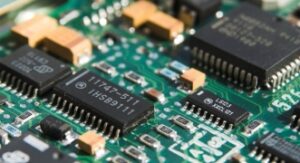
2026-03-12
View More >
2026-03-12
View More >