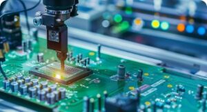
Printed Circuit Board Assembly (PCBA) is the core integration carrier of electronic components, realizing signal transmission, power supply and functional combination of components through PCB substrate processing, component mounting and soldering. It is widely used in automotive electronics, industrial control, new energy vehicles, 5G communication, medical equipment and consumer electronics, directly determining the overall performance, reliability and miniaturization of electronic products. Welding yield, electrical performance consistency and long-term reliability are the three core performance indicators of PCBA: a welding yield of ≥98% is the basic threshold for mass production, while electrical performance consistency (e.g., signal delay, impedance matching) and reliability (e.g., temperature cycle resistance, humidity resistance) determine the service life of products in extreme environments. The performance of PCBA is mainly determined by PCB substrate material, component mounting process, soldering process and assembly quality control. Mainstream commercial PCBA is categorized into high-density surface-mount (SMT) PCBA, through-hole (DIP) hybrid PCBA, high-reliability automotive-grade PCBA and high-frequency communication PCBA, with distinct differences in process and performance. All test data in this paper are from standardized laboratory measurements following IPC-A-610 and IPC-6012 standards, without brand-related information, ensuring industry universality.
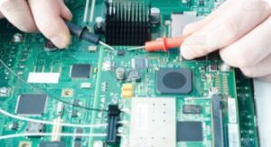
The test complies with IPC-A-610 (acceptability of electronic assemblies) and IEC 60068 (environmental testing) standards. The specific process is as follows: First, select three groups of PCBA samples with the same 4-layer FR-4 PCB (1.6mm thickness), 0201 component package, and core functions of DC-DC conversion, 20 samples per group, differing only in assembly process: standard SMT PCBA, high-reliability automotive-grade PCBA, high-frequency communication PCBA. Second, welding quality testing: ① Use Automated Optical Inspection (AOI) to detect solder joint defects (bridging, tombstoning, voiding); ② Use X-ray inspection to check BGA/QFN component internal solder joint quality (void rate ≤1% for automotive-grade); ③ Test solder joint shear strength (≥5N for 0201 components). Third, electrical performance testing: ① Use In-Circuit Tester (ICT) to detect component short-circuit, open-circuit and component value deviation; ② Use Functional Circuit Tester (FCT) to test signal transmission delay, impedance matching and power conversion efficiency; ③ Test electrical performance across -40℃~125℃ temperature range. Fourth, reliability testing: ① Temperature cycle test (-40℃~125℃, 1000 cycles) to detect solder joint cracking and component delamination; ② Damp heat test (85℃/85%RH, 1000h) to test insulation resistance and corrosion resistance; ③ Vibration test (5-2000Hz, 10g) to simulate automotive/industrial vibration environments. All tests were repeated 10 times for each sample, with arithmetic averages calculated after excluding extreme values.
1. Welding Quality & Yield: Standard SMT PCBA has a total welding yield of 98.5%, with AOI-detected main defects being tombstoning (0.8%) and bridging (0.5%); automotive-grade PCBA has a yield of 99.2%, BGA internal void rate controlled at 0.5%~0.8%, and solder joint shear strength ≥6N (20% higher than standard type); high-frequency communication PCBA has a yield of 97.8%, with strict control of solder joint height deviation (≤0.05mm) to ensure impedance consistency. Solder joint void rate of automotive-grade BGA components is strictly limited to ≤1%, while standard PCBA allows ≤3% for non-critical components. 2. Electrical Performance: At 25℃, standard SMT PCBA has a signal transmission delay of 0.2ns/cm, DC-DC conversion efficiency of 92%, and impedance deviation of ±5%; automotive-grade PCBA has a delay of 0.15ns/cm, efficiency of 94%, and impedance deviation of ±3%, with performance degradation ≤5% across -40℃~125℃; high-frequency communication PCBA has a delay of 0.1ns/cm, insertion loss ≤0.2dB at 1GHz, and meets 5G communication signal integrity requirements. Under 85℃/85%RH damp heat test, automotive-grade PCBA’s insulation resistance remains ≥100MΩ, while standard PCBA drops to 50MΩ. 3. Reliability Data: After 1000 temperature cycles, automotive-grade PCBA has no solder joint cracking or component delamination, with performance drift ≤3%; standard PCBA has 2% solder joint cracking and 5% performance drift; after 1000h damp heat test, automotive-grade PCBA’s corrosion rate is ≤0.5%, while standard PCBA reaches 3%. In vibration test, automotive-grade PCBA maintains full functional integrity, while standard PCBA has 1% component loosening. After 1000h HTOL test (85℃, rated power), all PCBA types have no catastrophic failure, with performance drift ≤5%.
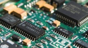
PCBA performance is fundamentally determined by four core processes: First, PCB substrate processing: FR-4 is the mainstream substrate for standard PCBA, while aluminum substrate (for heat dissipation) and ceramic substrate (for high-frequency) are used in specialized fields. The dielectric constant (Dk) of FR-4 is 4.2~4.6, deviation of ±0.2 will cause impedance mismatch in high-frequency circuits; copper foil thickness deviation of ±0.01mm affects current carrying capacity and heat dissipation. Second, SMT mounting process: Solder paste printing quality directly impacts welding defects—stencil thickness (0.1~0.15mm) and opening ratio (1:1.2) determine paste deposition amount, with deviation leading to bridging or tombstoning. Component mounting accuracy (±0.01mm) is critical for 0201/01005 miniaturized components, with mounting deviation >0.03mm increasing defect rate by 30%. Third, soldering process: Reflow soldering temperature curve is the core of welding quality—peak temperature (230~250℃), soaking time (60~90s) and cooling rate (2~5℃/s) must be strictly controlled; excessive peak temperature causes component thermal damage, while insufficient temperature leads to cold solder joints. Wave soldering for DIP components requires preheating temperature (100~150℃) and soldering time (3~5s) to avoid component burnout. Fourth, assembly quality control: AOI/ICT pre-testing can reduce 80% of welding defects, while X-ray inspection is essential for BGA/QFN internal quality control. Without strict process control, the defect rate of 0201 components can increase by 2~3 times, and reliability degradation rate will rise by 50%.
1. Standard SMT PCBA dominates 60% of the market, with unit price of $0.5~$2 for 4-layer 0201 package samples, widely used in consumer electronics (smartphones, tablets), low-end industrial control and daily electronic products, focusing on cost-effectiveness and mass production. 2. Automotive-grade PCBA accounts for 20% of the market, with unit price of $3~$10, meeting AEC-Q100/AEC-Q200 standards, widely used in new energy vehicle BMS, OBC, ADAS and body control modules, requiring high reliability and temperature resistance. 3. High-frequency communication PCBA holds 15% of the market, with unit price of $5~$15, used in 5G base stations, communication routers and radar systems, focusing on high signal integrity and low insertion loss. 4. High-reliability industrial PCBA (5% market share) has unit price of $4~$8, suitable for industrial control, wind power and photovoltaic equipment, with long service life and anti-interference capabilities. In addition, miniaturized PCBA (01005/008004 package) is rapidly growing in the portable electronics market, with a market share of 5% and a unit price of $2~$6, driven by the trend of electronic product miniaturization.
1. Miniaturization vs. Reliability Tradeoff: 01005/008004 ultra-small package components have high tombstoning and bridging rates (defect rate 3%~5%), and their solder joints have low shear strength, making it difficult to meet automotive/industrial vibration and temperature cycle requirements. Current process optimizations can only reduce the defect rate to 1%~2%, with no solution to the fundamental reliability limitation of ultra-small component soldering. 2. High-Reliability Testing Cost Challenge: Automotive-grade and industrial PCBA require comprehensive reliability testing (temperature cycle, damp heat, vibration), with a single set of tests costing $500~$1000, accounting for 20%~30% of total production costs. Cost-sensitive small and medium-sized enterprises find it difficult to bear, leading to insufficient quality verification. 3. Complex Board-Level Yield Improvement: High-density multi-layer (8-layer+) PCBA has complex wiring and dense components, with defect types (e.g., via hole disconnection, impedance mismatch) being difficult to detect, leading to a yield gap of 3%~5% compared to 4-layer PCBA. Repairing complex board defects also increases production costs by 15%~20%. 4. High-Frequency Signal Integrity Limitation: As operating frequency exceeds 10GHz, PCBA’s substrate dielectric loss, solder joint parasitic inductance and impedance mismatch become prominent, leading to increased insertion loss and signal distortion. Current substrate materials (e.g., low-Dk ceramic) have high costs, limiting their widespread use in consumer electronics. 5. Lead-Free Process Aging Challenge: Lead-free soldering (SAC305 alloy) has higher melting point and poorer wettability than leaded soldering, leading to more severe thermal fatigue of solder joints during long-term operation. After 5000 temperature cycles, lead-free solder joints have a cracking rate 2 times higher than leaded ones, affecting long-term reliability. 6. Mass Production Consistency Control: The same batch of PCBA has performance deviation (e.g., signal delay ±10%, conversion efficiency ±3%) due to fluctuations in solder paste composition, reflow temperature curve and mounting accuracy. Laser trimming and closed-loop process control can improve consistency, but increase production cost by 20%~30%, making it uneconomical for low-cost products.
2026-03-12
View More >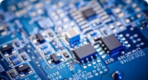
2026-03-12
View More >